Japan has made great progress in the use of printing methods to produce electronic components. The Japan Industrial Technology Research Institute, the University of Tokyo, Yamagata University, and the Tanaka Precious Metals Industry announced in April 2016 that they have developed the "SuPR-NaP method" (Surface PhotoReactive Nanometal Printing) based on the new principle. law). Using this technology, it is possible to realize the miniaturization, large area, and high-speed manufacturing of the wiring width and the like.
Compared with the conventional inkjet printing and screen printing, the SuPR-NaP method can reduce the width of wiring to a few tens of percent, and can also perform high-speed printing on a large flexible circuit board. As long as the processing temperature is 50 to 80° C., a resin having a lower heat-resistant temperature such as PET (polyethylene terephthalate) may be used as the substrate.
Tanaka Precious Metals will manufacture touch panel sensors based on a transparent conductive film made using this technology, and plans to supply samples from January 2017.
Beyond the previous transparent conductive film
The transparent conductive film produced by the new method surpasses the conventional technology in both light transmittance and sheet resistance (Fig. 1). This is because the wiring becomes finer and closer to the wavelength of visible light, so the reflectance decreases, and the wiring has higher conductivity than the conventional ink wiring.

Figure 1: Uniform wiring that achieves both high light transmittance and low sheet resistance
(a) Comparison of the light transmittance and the sheet resistance of the SuPR-NaP method with the current transparent conductive film. The closer to the upper left, the higher the performance of the transparent conductive film. The SuPR-NaP method has a light transmittance as high as 93% when the film resistivity is 20Ω/□. (b) Using the conventional coating method, a thick "coffee stain problem" such as a wiring may occur. (c) Any wiring width is processed using the SuPR-NaP method, and the thickness of the wiring is basically fixed.
The reason why the wiring has high conductivity is that the thickness in the longitudinal direction is very uniform and the thickness of the wiring cross-section is uniform. When the width is the same, the cross-sectional area of ​​the wiring is larger than in the prior art.
This is due to the SuPR-NaP method that solves the "coffee stain" problem that has plagued coating wiring. This is a problem of coating unevenness because the thickness of the wiring cannot be controlled, and the wiring width becomes large when it is desired to increase the thickness. The new technology can control the thickness of the wiring in the range of 30 to 100 nm.
Taking into account both the miniaturization and the large area
The miniaturization of wiring has been realized before. The "Super inkjet (SIJ) method", which was developed in 2002 by the Institute for Integrated Research, can print wiring with a width of about 1 μm. However, this method uses ultra-fine droplets to draw fine wirings one by one. The production speed is very slow and it is not suitable for mass production of large-area devices.
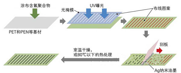
In contrast, the SuPR-NaP method uses ultraviolet light (UV) with a wavelength of 172 nm to uniformly draw the wiring pattern, and the ink coating can be performed simply by using a squeegee to sweep over the surface, and the miniaturization and large-area do not contradict each other. It is also very fast when making large area devices (Figure 2). The researchers produced an 8-inch (approximately 200mm) touch panel sensor. The UV exposure device with a wavelength of 172nm can use the "UV processor" that is used to remove organic substances on the surface of the LCD panel, and the manufacturing cost of the manufacturing equipment is also relatively low.

Figure 2: Scanning with a squeegee across the surface
Summary of SuPR-NaP coating process. First, fluoropolymers are applied to substrates such as PET and PEN. UV was irradiated from the top of the photomask, and the wiring pattern was fired. Silver silver ink is then coated with a squeegee, and only the silver nano-ink is left on the wiring pattern to form a wiring.
Use the difference in the binding force of the protecting group
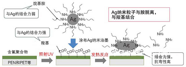
The new technology was able to achieve this breakthrough because it used the selective chemical adsorption of silver ink on the basis of the previous sparse control to fix the ink on the substrate where the wiring pattern was drawn (Fig. 3).

Figure 3: Silver nanoinks are chemically fixed onto a substrate
The SuPR-NaP method allows silver nanoinks to adhere to a substrate. After UV irradiation of the fluoropolymer, a large amount of carboxyl groups are formed on the surface. After the silver nanoparticles with the alkyl amine as the protective group are contacted with this, the carboxyl group with stronger silver binding will replace the alkyl amine and adsorb silver.
The sparsity control refers to a control technique in which a portion of the substrate having a wiring pattern has a high hydrophilicity and a pattern portion has a high hydrophobicity. In the past, most of the methods used were to place the ink on only a portion with high hydrophilicity, and there was a limit in controlling the wiring thickness and reducing the wiring width. Furthermore, the adhesion between silver and the substrate is poor, and the wiring may peel off from the substrate when the substrate is bent and stretched.
The new method is to apply a thin layer of fluoropolymer on the substrate and then draw the pattern by UV exposure. On the surface of the exposed fluoropolymer, a large amount of carboxyl groups will appear. The unexposed surface is highly hydrophobic, and after exposure, the hydrophobicity decreases slightly.
The silver ink used was developed by Professor Yoshihide Kurihara of Yamagata University, and Tanaka Precious Metals is promoting the production of this product. The ink encapsulates alkyl amine protecting groups in silver nanoparticles with a diameter of approximately 13 nm. The role of the protecting group is to prevent aggregation of the silver nanoparticles. In the past, most silver inks used carboxyl groups with strong silver binding. However, because of the strong binding force, after the silver ink is coated, the annealing temperature needs to be increased to remove the protective group.
The alkyl amine and the silver nanoparticles have weak binding force and can be replaced by carboxyl groups on the fluoropolymer after coating, so that the silver nanoparticles are fixed on the substrate. "The fixed adhesive force is 50 times the atmospheric pressure, that is, 5 MPa or more," said Hasegawa Duff, chief researcher of the Flextronics Research Center, which leads the development of this technology, and the professor of engineering of the Graduate School of Engineering at the University of Tokyo. Even if bent 100 times with a radius of curvature of 1mm, it will not peel off."
With the new technology, "coffee stains" no longer occur. The alkyl amine between the silver nanoparticles will fall off when heated to about 50-80°C, and the original annealing temperature should be above 100°C. (Reporter: Nozawa Tetsuo)
Food additives are substances added to food to preserve flavor or enhance its taste, appearance, or other qualities. Some additives have been used for centuries; for example, preserving food by pickling (with vinegar), salting, as with bacon, preserving sweets or using sulfur dioxide as with wines. With the advent of processed foods in the second half of the twentieth century, many more additives have been introduced, of both natural and artificial origin.
Food additives can be divided into several groups, although there is some overlap because some additives exert more than one effect. For example, salt is both a preservative as well as a flavor.
Sulfanlic Acid can be used as Food color for Lemon Yellow.
Food Coloring,Sulfanilic Acid For Food Color,Sulfanilic Acid For Food Additives
SJZ Chenghui chemical co ltd , https://www.chenghuichemicals.com